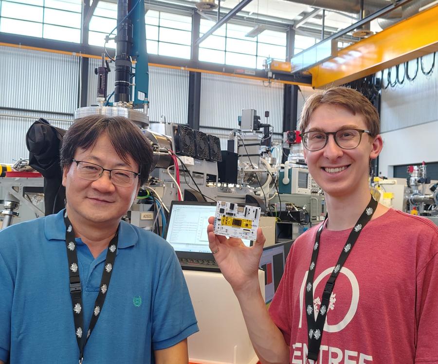
"ANSTO's microbeam facility offers exceptional ion-beam spatial resolution that is difficult to access elsewhere, enabling highly targeted radiation effects studies on advanced microelectronic devices. Equally important, the CAS team provides an outstandingly supportive and collaborative research environment, making complex experiments efficient and highly productive" - Prof Li Chen - University of Saskatchewan
The challenge
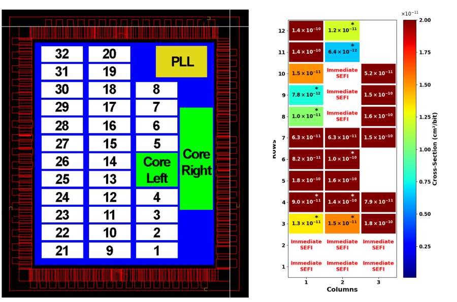
As integrated circuit technologies scale to deep-submicron nodes (12 nm and below), traditional broad-beam radiation testing methods lack the spatial resolution needed to accurately characterise single event effects (SEE) in increasingly complex devices. While pulsed lasers and ion microbeams offer high spatial precision, the correlation between results obtained using these techniques and those from standard broad-beam testing remains insufficiently understood. This gap limits confidence in applying laser and microbeam methodologies for space qualification, particularly for advanced digital systems such as radiation-hardened processors and memories. Addressing this challenge is critical to enabling reliable radiation assurance for next-generation space electronics.