
Technical Information - Platypus
Specifications, Instrument reference, User manual.


Showing 61 - 80 of 127 results
Specifications, Instrument reference, User manual.
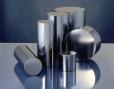
ANSTO is one of the world's leading providers of irradiation services for silicon ingots, which are used by the multimillion dollar electronics industry across Europe and Asia. Each year, ANSTO irradiates more than 50 tonnes of silicon.


Read about an ANSTO scientist and their work to prepare for a school project or interview.
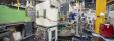
Kowari, a residual stress diffractometer, can be used for ‘strain scanning’ of large engineering components as large as 1000 kilograms.

Nick is a radiation biologist who works for the NST Human Health research theme.

The SAAFE Program supports early career researchers at PhD and Postdoctoral level to expand research and innovation activities within Human Health, the Environment and the Nuclear Fuel Cycle, to initiate sustainable research networks and linkages to support Australia, New Zealand and France research and innovation.

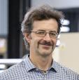
Role at ANSTO



Dr Karin Soldenhoff is a Principal Consultant within ANSTO's minerals area, managing the process development and research groups.

The BRIGHT Nanoprobe beamline provides a unique facility capable of spectroscopic and full-field imaging. NANO will undertake high-resolution elemental mapping and ptychographic coherent diffraction imaging. Elemental mapping and XANES studies (after DCM upgrade) will be possible at sub-100 nm resolution, with structural features able to be studied down to 15 nm using ptychography.

The growth and incorporation of graphene into semiconductor device architectures has been limited by challenges related to the quality, reproducibility, and high process temperatures required to grow it on suitable substrates.

ANSTO provides a summary of water usage and discharge for FY2024 - FY2025

A large group of ANSTO environmental scientists and collaborators have produced the first groundwater stable isotopes, ‘isoscapes’, intuitive maps with grid data, across NSW combining new and pre-existing isotope measurements.
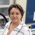
Dr Inna Karatchevtseva undertakes work at ANSTO in two main areas: defence industry research and fundamental materials research.